Semiconductor Physical Electronics - Teesside University
ORDER NEW SEMICONDUCTOR PHYSICAL ELECTRONICS ASSIGNMENT AT NOMINAL PRICE!
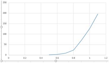
Question 1. The measured 1-V characteristics of a silicon high-speed diode (BAS 16) are given in TABLE 1, below.
(i) Plot a graph of the diode's forward characteristic.
Solution 1:
a) We simply draw a Diode forward I-V characteristics from the table
(ii) Compare the values of the diode's dynamic resistance and reverse current as obtained from TABLE 1 with those predicted by the diode equation. Attempt to account for any discrepencies.
Dynamic Resistance:
The ratio of change in voltage to the change in current is called dynamic resistance. It is denoted asR F.
RF = (Change in voltage)/(Change in current) = Δv/Δi
let we take the interval of Change in voltage from 0.8 to 1 and with respect we get the value of current 23mA to 127mA
by the definition we get
RF= (1 - 0.8)/(127mA - 23mA)
RF= 1.92 ohm
Reverse Resistance:
Resistance offered by the p-n junction diode when it is reverse biased is called Reverse resistance. The reverse resistance is in the range of mega ohms (MΩ).
RR= 75/1 uA
RR= 75 Mega Ohm
GET BENEFITTED WITH QUALITY SEMICONDUCTOR PHYSICAL ELECTRONICS ASSIGNMENT HELP SERVICE OF EXPERTSMINDS.COM
Question 2.
(a) Describe how 'depletion-layer'capacitance arises in a pn junction and identify three parameters that control its value. Give an application for a variable-capacitance diode.
Solution (a):
We know that the equation for the capacitance and it relation with the depletion layer is
C = (∈A)/W
C= Total Capacitance of the junction
A= Cross sectional area
?= Permittivity or semiconductor
Wd= Width of depletion region
Parameters that control depletion layer capacitance:
1- Reverse voltage
When the reverse voltages increase the capacitance decreases and width of depletion layer increases and vice versa and with of depletion layer also depend on number of impurities added.
2- Width is directly proportional Area:
Hence the cross-sectional area increase cause depletion region increases
3- Width is directly proportional E(permittivity)
4- Hence the value of permittivity increase cause depletion region increases
(b) Question
In an experiment to determine the temperature dependence of the reverse saturation current, Is of a selected diode was measured at different temperatures. The results are given in TABLE B. The diode (1N4001) has an ideality factor of N = 1.90.
Solution: By the given formula we can find the value of Energy Gap WG.
|
T.C
|
ISnA
|
WG
|
|
20
|
16
|
9.41×10⁻²¹
|
|
25
|
26
|
1.14×10⁻²⁰
|
|
30
|
33
|
1.35×10⁻²⁰
|
|
35
|
53
|
1.53×10⁻²⁰
|
|
40
|
73
|
1.72×10⁻²⁰
|
|
45
|
106
|
1.89×10⁻²⁰
|
ORDER NEW COPY OF SEMICONDUCTOR PHYSICAL ELECTRONICS ASSIGNMENT & GET HIGH QUALITY SOLUTIONS FROM SUBJECT'S TUTORS!
Question 3. (a) Explain, with the aid of diagrams, the design features of a rectifier diode that enables it to have both a high current and high reverse-voltage rating. Your answer should make reference to device geometry, choice of materials and levels of doping. (Note that up-to-date information is available in manufacturers' data books and on the intemet.)
Solution:
Rectifier diode is simple diode which have pnjunction, p type impurities and n type as well. Let if we take an example of 1N4007 Diode we know that is it has a high forward current of 10A and high reverse voltage 700V
Because it has following features
• low leakage current
• low voltage drops
• high junction temperature up to 150 degree
• maximum blocking DC voltages
these feature enables the diode to operate on high current and high reverse voltage rating.
(b) A particular diode and its associated heat sink have the characteristics and ratings listed below. Calculate the maximum ambient temperature at which the diode can safely operate.
Solution
Tj= Ta+ Rth
Ta=Tj - Rth
Rth = Rj-c + Rc-s
= 7 KW-1+ 0.5 KW-1
= 7.5KW-1
= 200oC - (7.5 °C/w) (IF×VF)
= (200 -147) °C
Ta = 53°C
DO YOU WANT TO EXCEL IN SEMICONDUCTOR PHYSICAL ELECTRONICS ASSIGNMENT - ORDER AT EXPERTSMINDS!
(c) Explain how metal-to-semiconductor junctions may be ohmic or rectifying.
Solution:
Metal semiconductor is defined as "When aluminum or platinum metal is joined with N-type semiconductor, a junction is formed between the metal and N-type semiconductor. This junction is known as a metal-semiconductor junction or M-S junction".A junction formed between a n-type semiconductor metal creates adepletion region and barrier calledmetal semiconductor(M-S)
The M-S junction can rectify or ohmic contact.
If it is non-rectifying metal-semiconductor junction is called ohmic contact.
In Ohmic Contact themetal-semiconductor junction offers very low resistance that's why it behaves as ohmic whereas the rectifying metal-semiconductor junction offers high resistanceand it behaves as rectifying.
(d) Identify the properties of a Schottky type junction which give it applications in both low power integrated circuits and very high power discrete devices.
Solution:
property and advantages of the Schottky diode is given below
• It has Low junction capacitance
• Schottky diode has Fast reverse recovery time
• High current density
• Low forward voltage drops
• Schottky diode has high efficiency
• Having high frequencies.
• The noise between the PN junction of Schottky diode is less
These properties make them to use in low power circuits and high-power circuits as well.
SAVE TOP GRADE USING SEMICONDUCTOR PHYSICAL ELECTRONICS ASSIGNMENT HELP SERVICE OF EXPERTSMINDS.COM
Question 4. FIGURE 1(a) shows a power supply using a full-wave bridge rectifier circuit. The mains supply is stepped down by the transformer T1 and the secondary voltage Vs rectified by the four diodes D1 -D4; diodes Dl and D3 conduct on one half cycle and D2 and D4 on the other. The diodes are provided in a single 4-pin bridge-rectifier package which can be mounted directly onto a printed circuit board.
Solution:
From this fig we simply observe that our
Vp=240 v
Turn ratio =10:1
Vs=24V
Which after passing through Bridge rectifier
Vdc=2vm/pi
V r =15.2 v
RL=30
So, Load Current we get is IL=0.5 A
And fuse has a rating of 3A.
So, if we want to select the rectifier from the given tablewe choose
type D Because it is rule of thumb that we choose that rectifier by viewing transformer secondary voltage 24 * 3 = 72
So, if B has voltage rating 24V we choose the type D it has voltage rating 72 volt and current is 4 A.
DONT MISS YOUR CHANCE TO EXCEL IN SEMICONDUCTOR PHYSICAL ELECTRONICS ASSIGNMENT! HIRE TUTOR OF EXPERTSMINDS.COM FOR PERFECTLY WRITTEN SEMICONDUCTOR PHYSICAL ELECTRONICS ASSIGNMENT SOLUTIONS!!
UK assignment help offered for various courses and programs offered at Teesside University:
- Microprocessor Systems Assignment Help
- Programmable Logic Controllers Assignment Help
- Semiconductor Structure and Fabrication Assignment Help
- Business Management Techniques Assignment Help
- Combinational and Sequential Logic Assignment Help
- Control Systems and Automation Assignment Help
- Electrical Supply and Distribution Assignment Help
- Electrical Systems Protection Assignment Help
- Electromagnetic Compatibility Assignment Help
- Engineering Design Assignment Help