Semiconductor Physical Properties Assignment Questions -
ARE YOU LOOKING FOR RELIABLE SEMICONDUCTOR PHYSICAL PROPERTIES ASSIGNMENT HELP SERVICES? EXPERTSMINDS.COM IS RIGHT CHOICE AS YOUR STUDY PARTNER!
Question 1 - In an experiment, the current through and the voltage across the opposite faces of three specimen blocks of material, each 1 cm3, was measured using the circuit of FIGURE 1. Use the results of the experiment, given in the table below, to classify each material as insulator, conductor or semiconductor.
Answer - It is given in the question the voltage and current values of three specimens as follows
|
Specimen
|
V
|
I
|
|
A
|
10V
|
40µA
|
|
B
|
10V
|
0.2A
|
|
C
|
1000V
|
10nA
|
The length breadth and width of the material are 1cm each.
To check the given materials are insulators, conductors and semiconductors we can calculate the resistivity.
Resistivity ρ = RA/l
We know R = V/I
A = 1cm2 and length = 1cm
So
|
Specimen
|
V
|
I
|
R = V/I
|
ρ = RA/l
|
|
A
|
10V
|
40µA
|
10/(40 x 10-6) = 250kΩ
|
=(250 x 103 x 1)/1 = 250 x 103 Ωcm
|
|
B
|
10V
|
0.2A
|
10/0.2 = 50Ω
|
(50 x 1)/1= 50 Ωcm
|
|
C
|
1000V
|
10nA
|
1000/(10 x 109) = 100 x 109 Ω
|
= (100 x 109 x 1)/1 = 100 x 109 Ωcm
|
Based on these values
|
Specimen
|
Materials
|
|
A
|
Semiconductor
|
|
B
|
Conductor
|
|
C
|
Insulator
|
DO YOU WANT TO EXCEL IN SEMICONDUCTOR PHYSICAL PROPERTIES ASSIGNMENT - ORDER AT EXPERTSMINDS!
Question 2 (i) - Sketch and label energy-band diagrams of a metal, an insulator and a semiconductor and give approximate values of the energy gap where appropriate.
Answer - Energy band diagram
1 eV = 1.6 × 10⁻¹⁹J
|
Materials
|
Energy band diagram
|
Band gap values
|
|
Insulator
|
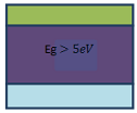
|
Energy gap value is greater than 5eV
|
|
Semiconductor
|
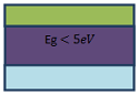
|
Energy gap less than 5e V
|
|
Metal
|

|
Band gap will overlap.
|
Question 2 (ii) - The three graphs of FIGURE 2 show how the resistivities of metals, insulators and intrinsic semiconductors vary over a small temperature range. Explain the shape of the graphs in terms of the energy-band theory of electrons in solids.
Answer - We can explain as follows
|
Materials
|
Explanation
|
|
Metal
|
Metals are having low resistivity. When the temperature is increased the resistivity is also increased. Metals have positive temperature coefficient.
|
|
Insulator
|
Insulators are having high resistivity. When temperature is increased the resistivity will decrease, showing the negative temperature coefficient.
|
|
Intrinsic Semiconductor
|
Intrinsic semiconductors are having the greatest resistivity. When the temperature is increased the resistivity will decrease, showing negative temperature coefficient.
|
HIRE PROFESSIONAL WRITER FROM EXPERTSMINDS.COM AND GET BEST QUALITY SEMICONDUCTOR PHYSICAL PROPERTIES ASSIGNMENT HELP AND HOMEWORK WRITING SERVICES!
Question 3 (i) - Determine the current flowing through a 1 cm cube of pure silicon when a potential of 1 V is applied across opposite faces (FIGURE 3(a)) if the number density of hole-electron pairs in the cube 1.56 x 10¹⁶ m-3.
Answer - We need to determine the current flowing
As we know the resitivity is ρ = RA/l
R = ρl/A
V/I = ρl/A = l/Aσ = l/Aqdesity
= (1×10⁻²)/(1×10-6 × 1.6×10-19 × 1.56×1016)
I = (1×10-6 × 1.6×10-19 × 1.56×1016)/(1×10-2)
I = 2.496×10⁻⁷A
= 0.2496µA
Question 3 (ii) - A lamp is now allowed to shine upon one face of the cube as shown in FIGURE 3(b). This has the effect of generating hole-electron pairs at the surface of the exposed face and so raising the number densities of the carriers at that surface to a value of 1 x 10²⁰ carriers m-3. For the polarities of external connections as shown, calculate the change in hole current due to the effects of the light.
Answer - We need to determine the current flowing
As we know the resitivity is ρ = RA/l
R = ρl/A
V/I = ρl/A = l/Aσ = l/Aqdesity
= (1×10⁻²)/(1×10-6 × 1.6×10-19 × 1×1020)
I = (1×10-6 × 1.6×10-19 × 1×1020)/(1×10-2)
I = 1.6×10⁻³ A
= 1.6mA
Question 3 (iii) - If the polarity of the supply is now reversed, calculate the change in electron current due to the light. Again, assume a linear density gradient.
Answer - If the polarity is reversed then the current will change its direction as -1.6mA.
MOST RELIABLE AND TRUSTWORTHY SEMICONDUCTOR PHYSICAL PROPERTIES ASSIGNMENT HELP & HOMEWORK WRITING SERVICES AT YOUR DOORSTEPS!
Question 4 - Use the Fermi-Dirac probability function
p(W) = (1+ exp((W-WF)/kT))-1
to calculate, for pure silicon at a temperature of 27oC, the probability of:
(a) an electron just being at the bottom of the conduction band
Answer - Electron at the bottom of conduction band
w-wF = 0
so exp[(w-wF)/KT] = 1
p(w) = (1+1)-1 = ½5
(b) A hole just being at the top of the valence band.
Answer - Hole at the top of conduction band
w-wF = 0
so exp[(w-wF)/KT] = 1
p(w) = (1+1)-1 = 1/2
Question 5 - A silicon 'chip' has the dimensions 8 x 2 x 2 mm.
(i) Calculate its resistance as measured between the square faces, assuming it is of intrinsic material. Take the carrier number density of hole-electron pairs as 1.5 x 10¹⁶ m-3 at room temperature.
Answer - We need to calculate the resistance
Given that a pure si at absolute temperature
So σ = q(μn + μp)ni
We know the values of μn + μp = 0.15 + 0.05 = 0.2
Now σ = 1.6×10-19 × 0.2×1.5×1016
= 0.48×10⁻³
Now ρ = (σ)-1
ρ = 2083
R = ρl/A = (2083×8×10-3)/(16×10-6) = 10.4MΩ
(ii) Estimate its resistance at 10oC above room temperature.
Answer - Resistance at 10oC above room temperature
Almost same as 10.4MΩ because the si sample is not doped at this temperature.
(iii) Calculate the resistance, again across the square faces and at room temperature, if the 'chip' is now uniformly doped with aluminium, so that one in every 107 atoms is an impurity atom (a cubic metre of silicon contains about 5 x 1028 atoms). Also apply the 'law of mass action' to calculate the minority carrier density.
Answer - σ = q(μnno + μppn)
Given that n0 = 5×1028
Now po = (ni2)/n0 = 5120
Now σ = 1.6×10⁻¹⁹[0.15×5×1028 + 0.5×5120]
= 12×108
Now ρ = (σ)-1
ρ = 0.0833×10⁻⁸
R = ρl/A = (0.0833×10-8×8×10-3)/(16×10-6) = 0.042×10⁵Ω
(iv) Estimate the resistance of the doped 'chip' at 10oC above room temperature.
Answer - When temperature is greater than room temperature the resistance will have slight variations.
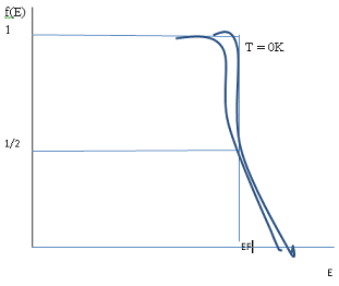
(v) Sketch, on the same axes, the energy/probability distribution curve for n-type silicon at two temperatures T1 and T2 (where T2 > T1) to show the effect of temperature upon the position of the Fermi level.
Answer - The diagram is as below
Acquire our Teesside University course help and assignment help services for various related courses such as: -
- Analytical Methods for Engineers Assignment Help
- Engineering Science Assignment Help
- Electrical and Electronic Principles Assignment Help
- Project Assignment Help
- Applications of Pneumatics and Hydraulics Assignment Help
- Digital and Analogue devices and circuits Assignment Help
- Distributed Control Systems Assignment Help
- Electrical machines Assignment Help
- Engineering Applications Assignment Help
- Mechatronics Systems Principles Assignment Help